MATERIALS.IE
Metals • Plastics • Rubbers • Polymers • Ceramics • Composites
Metals • Plastics • Rubbers • Polymers • Ceramics • Composites
Metals • Plastics • Rubbers • Polymers • Ceramics • Composites • Coatings
ELECTRONIC MATERIALS & CONNECTORS
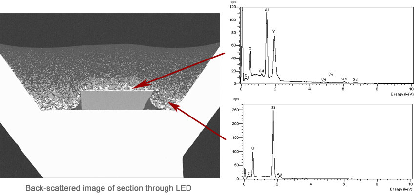
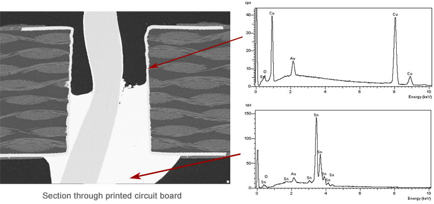
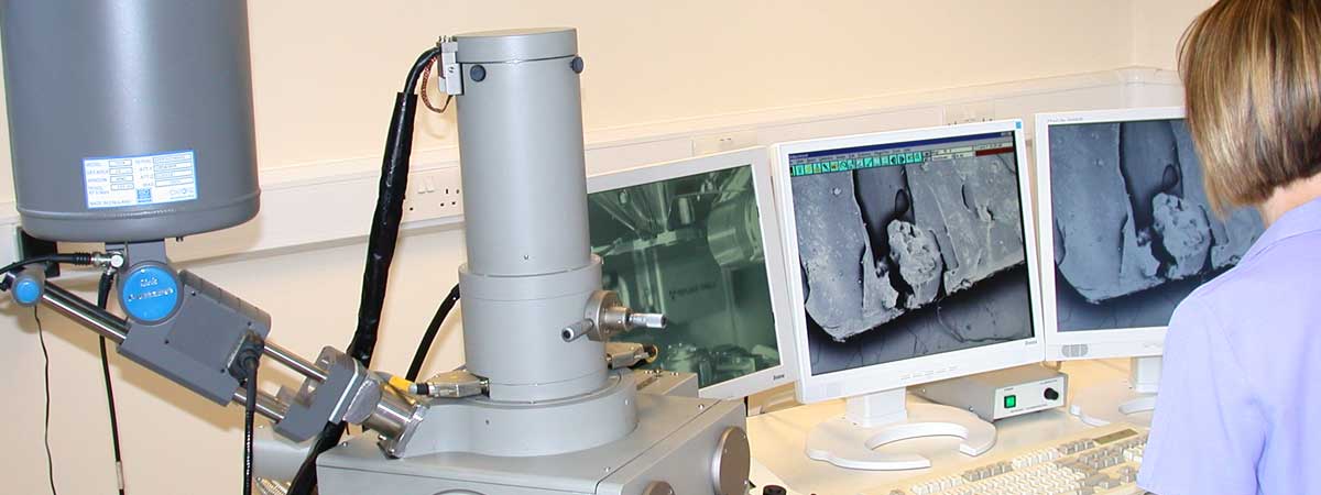
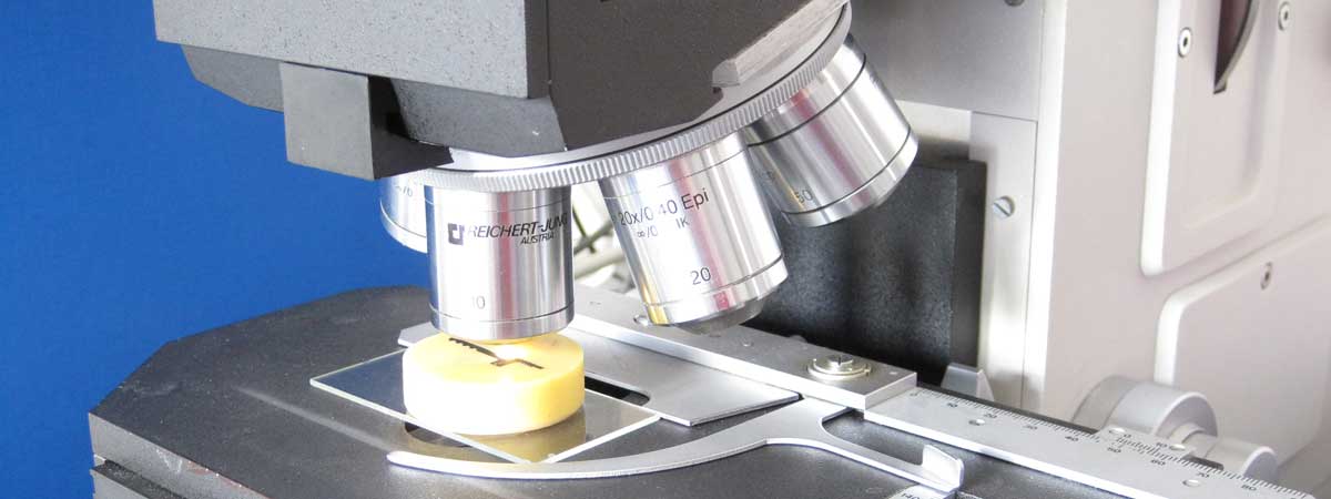
Analysis of individual electronic components, connectors and printed circuit boards by scanning electron and optical microscopy, including cross-sectional examination, can assist investigation of failures and potential areas of failure.Cross sectioning and ultra-high magnification imaging with x-ray analysis of PCBs, connectors and components can reveal details including:
- composition and thickness of plating layers and interlayers,
- through hole plating/vias,
- contamination including lead,
- environmental factors such as chemical attack/corrosion,
- damage to contact faces and layers, including fretting/oxidation,
- cyclic failure/fatigue,
- fracture of solder joints.